

Working Group: Materials and Interfaces
With their decisive role for numerous natural and technological processes which range from nanoelectronics, sensor technology, solid state lighting, catalysis and solar conversion, surfaces and interfaces dominate most physicochemical processes occurring within functional nanomaterials. Interfaces can be engineered to tune the function and stability of nanostructures, but also induce complex assembly at the meso- and the microscale, providing access to a range of new materials.
The group has profound expertise in functional properties of local surface and interfaces within nanostructured solids. This includes:
- characterization and engineering of defects and impurities in metal oxide nanostructures,
- study of charged surfaces in the context of photoelectrochemical applications,
- metal/semiconductor and plasmonic materials.
Various methods are employed to generate pure and nanoparticle composites in the form of dry powders, colloidal dispersions or thin nanostructured films with specific chemical, optical and electronic properties. Furthermore, our research aims at the understanding of growth and stability of these metastable nanoscale solids in order to determine their potential use and reliability under realistic operation conditions.
Methods
Powders and colloids as well as dense and porous thin films are prepared by gas-phase and wet-chemical synthetic strategies (chemical vapor synthesis, hydrothermal synthesis, thin film deposition by DC and RF sputtering, electrophoretic thin film deposition, electrochemical deposition within porous membranes, nanosphere lithography, metal assisted chemical etching).
Following synthesis the materials are processed in a controlled way (e.g. by thermal sample activation in defined atmospheres to obtain clean surfaces) and transferred into defined environments (high vacuum conditions, gas atmospheres, liquids and electrolytes). Compositional and microstructural materials properties are studied by a combination of spectroscopic methods (UV/Vis spectroscopy in transmission and diffuse reflectance, IR spectroscopy in transmission and attenuated total reflection), electron microscopy (SEM and TEM including elemental analysis and electron diffraction) as well as techniques for the characterization of colloidal properties (dynamic light scattering, laser Doppler electrophoresis).
Defect generation as well as recombination, transport and transfer of charge carriers are studied by a combination of spectroscopic (photoluminescence, electron paramagnetic resonance, cathodoluminescence), electric (4-point probe measurements, electron-beam induced current measurements) and electrochemical techniques (IR and UV/Vis spectroelectrochemistry, photoelectrochemistry).
The materials performance is evaluated by determining e.g. the photoluminescence quantum yield at particle powders and colloids or the external and internal conversion efficiencies of photoelectrodes.
Selected publications:
- Defects in Oxide Particle Systems, T. Berger and O. Diwald, in “Defects on Oxide Surfaces” edited by J. Jupille, G. Thornton, Springer Series on Surface Science, Vol 58, Pages 273-301 (2015)
- Traps and Interfaces in Photocatalysis: Model Studies on TiO2 Particle Systems, T. Berger and O. Diwald in Photocatalysis Fundamentals and Perspectives, RSC Energy & Env. Series No. 14,: ed. Jenny Schneider, Detlef Bahnemann, et al., p 185-215, in press, © The Royal Society of Chemistry 2016
- Interfaces in nanocrystalline Oxide Materials: from Powders towards Ceramics, O. Diwald, K. P. McKenna, A. L. Shluger, in “Computational Modeling of Inorganic Nanomaterials” edited by S. T. Bromley, M. Zwijnenburg; CRC Press, ISBN-13: 978-1466576414 , in press (2016)
- The Electrochemistry of Nanostructured Titanium Dioxide Electrodes, T. Berger, D. Monllor-Satoca, M. Jankulovska, T. Lana-Villarreal, R. Gómez ChemPhysChem 2012, 13, 2824-2875.
Team
- DIWALD Oliver, Univ. Prof. Dr. (head)
- BERGER Thomas, Assoz. Prof. Dr.
- Bourret Gilles R., Assoz. Prof. Dr.
- AICHER Korbinian, MSc.
- BARTSCHMID Eva Theresa, BSc.
- NEIGE Ellie, Dipl.-Chem.
- PIASKOWSKI Joshua, MSc.
- RAZOUQ Hasan, MSc.
- SCHWAB Thomas, MSc.
Research Themes:
Stability and transformation of non – equilibrium solids

Nanostructures typically form under kinetic control. The structural and compositional relaxation/ reorganization pathways these metastable solids undergo toward their equilibrium state are often not understood. Understanding such processes is crucial to control stability and performance of functional nanostructures in devices.
Selected Publications:
- Thin Water Films and Magnesium Hydroxide Fiber Growth; A. Gheisi, A. Sternig, G.J. Redhammer, and O. Diwald*; RSC Advances, 5 (2015) 82564-82569.
- Morphology and photoelectronic Properties of layered Titanate Nanostructures, A. Riss, M.J. Elser, J. Bernardi, O. Diwald, J. Am. Chem. Soc., 131 (2009) 6198–6206.
- Nanoparticles as Support: CaO Deposits on MgO Cubes, M. Müller, A. Sternig, S. Stankic, M. Stöger-Pollach, J. Bernardi, E. Knözinger, O. Diwald; J. Phys. Chem. C, 112 (2008) 9120-9123
Interfacing Nanostructures

When discussing how the chemical and physical properties of nanoparticle powders differ from those of macroscopic materials, it is common to point to their high specific surface area, the size and shape of the constituent nanocrystals, and the high concentration of surface features, such as steps, kinks, and other low coordination sites. Another defining characteristic of this type of materials is the large number of interfaces between nanocrystals they contain. However, the beneficial and/ or detrimental influence of interfaces on the overall properties of nanoparticle powders has not been studied and is only rarely understood. In this project we explore different possibilities to selectively generate these interfaces and to directly address them by chemistry, light or thermal materials processing. Related activities aim at new means for functionalization and chemical activation of oxide nanostructures and, consequently, at improving performance and reliability for many nanoparticle powder applications.
Selected Publications:
- Traps and Interfaces in Photocatalysis: Model Studies on TiO2 Particle Systems, T. Berger and O. Diwald in Photocatalysis Fundamentals and Perspectives, RSC Energy & Env. Series No. 14,: ed. Jenny Schneider, Detlef Bahnemann, et al., p 185-215, in press, © The Royal Society of Chemistry 2016
- Porphyrin Metalation at MgO Surfaces: A Spectroscopic and Quantum Mechanical Study on Complementary Model Systems; J. Schneider, M. Franke, M. Gurrath, M. Röckert, T. Berger, J. Bernardi, B. Meyer*, H.-P. Steinrück, O. Lytken*, and O. Diwald*; Chem Eur. J. 22 (2016) 1744 – 1749.
- Optical Properties of Nanocrystal Interfaces in Compressed MgO Nanopowders K. McKenna, D. Koller, A. Sternig, N. Siedl, N. Govind, P.V. Sushko, and O. Diwald, ACS Nano, 5 (2011) 3003-3009.
- Particle Networks from Powder Mixtures: Generation of TiO2-SnO2 Heterojunctions via Surface Charge-Induced Heteroaggregation, N. Siedl, S. O. Baumann, M. J. Elser, and O. Diwald*, J. Phys. Chem. C 116 (2012) 22967-22973.
Doping, Decoration and impurity admixture

In oxide nanostructures compositional heterogeneity can range from impurity doping of the host lattice to phase separated nanocomposites with multifunctional properties. In this project we aim at the assessment of wanted and unwanted properties of extrinsic defects as well as materials alloying and segregation effects at the nanoscale.
Selected Publications:
- Solar Light and Dopant induced Recombination Effects in TiO2: photoactive Nitrogen as a Case Study, M. D’Arienzo, R. Scotti, F. Morazzoni, N. Siedl, A. Sternig, J. Bernardi, and O. Diwald; J. Phys. Chem. C 114 (2010) 18067-18072.
- Surface-specific visible Light Luminescence from composite Metal Oxide Nanocrystals; A. Sternig, J. Bernardi, K. Mc Kenna*, and O. Diwald*, J. Mater. Sci. 50 (2015) 8153-8165.
- Phase Separation at the Nanoscale: structural Properties of BaO Segregates on MgO-based Particles; A. Sternig, S. Klacar, J. Bernardi, M. Stöger-Pollach, H. Grönbeck, and O. Diwald, J. Phys. Chem. C, 115 (2011) 15853-15861.
Growth and organization of nanomaterials

Beginning from intense research on size effects specific to individual nanoscale building blocks the need to arrange metal oxide nanoparticles at the meso- and macroscale has emerged as an important and urgent research topic in current nanoscience. This includes the assembly of nanoscale building blocks over several lengths scales from the nano- to the centimeter range retaining the nanoscale properties in the final macroscopic object or device. As a matter of fact interfaces between the nanoobject and surrounding materials environment emerge from this materials organization step. This project aims at the elucidation of how growth and microstructure evolution different types of interfaces impact the overall ensemble properties in terms of microstructure, optical, electronic and chemical properties.
Selected Publications:
- On the entangled Growth of NaTaO3 Cubes and Na2Ti3O7 Wires in Sodium Hydroxide Solution, S.O. Baumann, C. Liu, M.J. Elser, A. Sternig, N. Siedl, T. Berger, O. Diwald*, Chemistry – A European Journal, 19 (2013) 10235-10243.
- Defects in Oxide Particle Systems, T. Berger and O. Diwald, in “Defects on Oxide Surfaces” edited by J. Jupille, G. Thornton, Springer Series on Surface Science, Vol 58, Pages 273-301 (2015)
- Solid-Solid Interface Formation in TiO2 Nanoparticle Networks; S. Baumann, N. Hüsing, M.J. Elser, O. Diwald, Langmuir 27 (2011) 1946-1953.
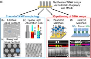
Nanophotonics
Metal and semiconductor nanostructures have a strong and tunable interaction with light, which can be used to significantly enhance surface and bulk electric fields (E-fields). By engineering heterostructures down to the nanometer scale, we control E-field enhancements and light absorption in three-dimensions, which are optimized for surface-enhanced Raman spectroscopy (SERS, i.e. chemical sensing), and photocatalysis.
Selected recent publications:
• „Dewetting-Assisted Patterning: A Lithography-Free Route Synthesis of Black and Colored Silicon“ A. Farhadi, T. Bartschmid and G. R. Bourret ACS Appl. Mater. Interf., 2023, 15, 44087–44096
• „Large-Scale Synthesis of Highly Uniform Silicon Nanowire Arrays using Metal-Assisted Chemical Etching (MACE)“ F. Wendisch, M. Rey, N. Vogel, G. R. Bourret Chemistry of Materials 2020, 32, 9425–9434.
• „Three-Dimensional Electrochemical Axial Lithography“, F. J. Wendisch, M. S. Saller, A. Eadie, A. Reyer, M. Musso, M. Rey, N. Vogel, O. Diwald, G. R. Bourret Nano Letters 2018, 18, 7343-7349.
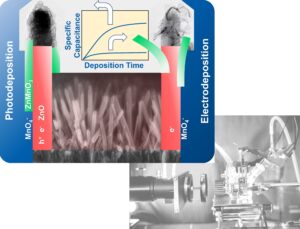
Synthesis of electro- and photoactive films
Low-temperature chemical, photochemical and electrochemical deposition strategies are developed in our group to directly grow electro- and photoactive nanostructured semiconductor oxide films onto suitable substrates. The synthetic realization of single- and multi-phase films featuring complex but tunable composition and morphology relies on controlling the reactivities of dissolved precursor species, of the substrate material and of the newly formed phase. By properly tuning the crystallographic relationship between substrate and deposit, these strategies furthermore aim at the growth of metastable phases, which are not accessible via high-temperature preparation processes (e.g. electrodeposition of the defective cubic spinel ZnMnO3 at the surface of ZnO nanowires).
Selected publications:
Rettenmaier, K., Zickler, G.A., Berger, T. Conformal Coverage of ZnO Nanowire Arrays by ZnMnO3: Room-temperature Photodeposition from Aqueous Solution (2023) ChemPhysChem, 24 (21), e202300250. DOI: 10.1002/cphc.202300250
Rettenmaier, K., Zickler, G.A., Redhammer, G.J., Berger, T. Substrate-Enabled Room-Temperature Electrochemical Deposition of Crystalline ZnMnO3 (2023) ChemPhysChem, 24 (1), e202200586. DOI: 10.1002/cphc.202200586
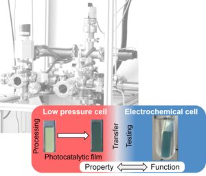
Processes at the semiconductor/electrolyte interface
To study processes at solid/liquid interfaces we apply and develop advanced in situ characterization methods. Examples include the use of electrochemical impedance spectroscopy, IR- and UV/Vis-spectroscopy to study bias- or light-induced processes at the semiconductor/electrolyte interface. Only recently, a dedicated reactor system was developed, which allows (i) to process nanostructured oxide films in defined gas atmospheres in a low pressure chamber (activation/processing cell) and (ii) to transfer the processed samples under inert conditions (i.e. without passing through the ambient atmosphere) into a liquid electrolyte solution and use them as electrodes in a (photo)electrochemical cell (high pressure chamber). The impact of processing-induced property changes on electrode performance can thus be studied in a systematic way. This has been exploited, for instance, to elucidate, how the photoelectrocatalytic activity of WO3 and TiO2 nanoparticle electrodes can be optimized via chemical reduction of the semiconductors by atomic hydrogen.
Selected publications:
Jiménez, J.M., Zickler, G.A., Redhammer, G.J., Berger, T. Chemical reduction of porous WO3 and TiO2 photoelectrocatalysts by atomic hydrogen (2023) Appl. Catal. A, 658, 119163, DOI: 10.1016/j.apcata.2023.119163
Rettenmaier, K., Zickler, G.A., Redhammer, G.J., Anta, J.A., Berger, T. Particle Consolidation and Electron Transport in Anatase TiO2 Nanocrystal Films (2019) ACS Appl. Mater. Interfaces, 11 (43), 39859-39874. DOI: 10.1021/acsami.9b12693


